- 您现在的位置:买卖IC网 > Sheet目录328 > IDT7014S12JG (IDT, Integrated Device Technology Inc)IC SRAM 36KBIT 12NS 52PLCC
IDT7014S/L
High-Speed 4K x 9 Dual-Port Static RAM
AC Electrical Characteristics Over the
Operating Temperature and Supply Voltage
Industrial and Commercial Temperature Ranges
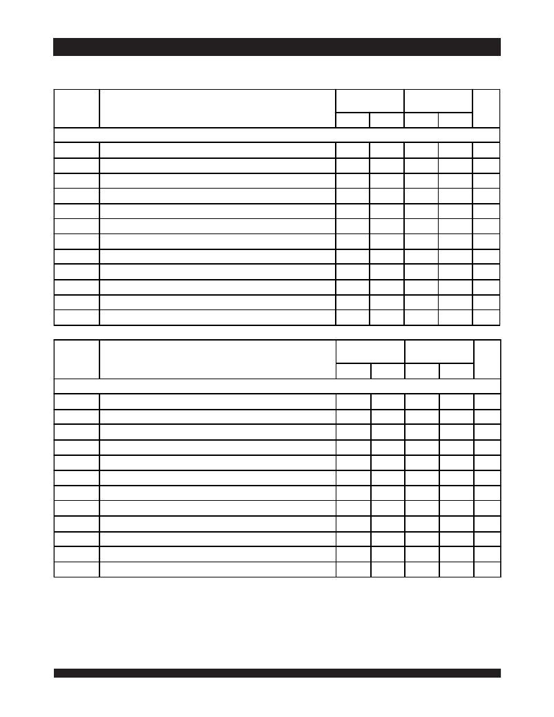
7014S12
Com'l Only
7014S15
Com'l Only
Symbol
Parameter
Min.
Max.
Min.
Max.
Unit
WRITE CYCLE
t WC
t AW
t AS
t WP
t WR
t DW
Write Cycle Time
Address Valid to End-of-Write
Address Set-up Time
Write Pulse Width
Write Recovery Time
Data Valid to End-of-Write
12
10
0
10
1
8
____
____
____
____
____
____
15
14
0
12
1
10
____
____
____
____
____
____
ns
ns
ns
ns
ns
ns
t HZ
Output High-Z Time
(1,2)
____
7
____
7
ns
t DH
Data Hold Time
(3)
0
____
0
____
ns
t WZ
t OW
Write Enable to Output in High-Z (1,2)
Output Active from End-of-Write (1,2,3)
____
0
7
____
____
0
7
____
ns
ns
t WDD
Write Pulse to Data Delay
(4)
____
25
____
30
ns
t DDD
Write Data Valid to Read Data Delay
(4)
____
22
____
25
ns
2528 tbl 09a
7014S20
Com'l & Ind
7014S25
Com'l Only
Symbol
Parameter
Min.
Max.
Min.
Max.
Unit
WRITE CYCLE
Write Enable to Output in High-Z
t WC
t AW
t AS
t WP
t WR
t DW
t HZ
t DH
t WZ
Write Cycle Time
Address Valid to End-of-Write
Address Set-up Time
Write Pulse Width
Write Recovery Time
Data Valid to End-of-Write
Output High-Z Time (1,2)
Data Hold Time (3)
(1,2)
20
15
0
15
2
12
____
0
____
____
____
____
____
____
____
9
____
9
25
20
0
20
2
15
____
0
____
____
____
____
____
____
____
11
____
11
ns
ns
ns
ns
ns
ns
ns
ns
ns
t OW
Output Active from End-of-Write
(1,2,3)
0
____
0
____
ns
t WDD
t DDD
Write Pulse to Data Delay (4)
Write Data Valid to Read Data Delay (4)
____
____
40
30
____
____
45
35
ns
ns
NOTES:
2528 tbl 09b
1. Transition is measured 0mV from Low or High-impedance voltage with Output Test Load (Figure 2).
2. This parameter is guaranteed by device characterization, but is not production tested.
3. The specification for t DH must be met by the device supplying write data to the RAM under all operating conditions. Although t DH and t OW values will vary over voltage
and temperature, the actual t DH will always be smaller than the actual t OW .
4. Port-to-port delay through RAM cells from writing port to reading port, refer to “Timing Waveform of Write With Port-to-Port Read”.
7
6.42
发布紧急采购,3分钟左右您将得到回复。
相关PDF资料
IDT7015L35G
IC SRAM 72KBIT 35NS 68PGA
IDT7016L35G
IC SRAM 144KBIT 35NS 68PGA
IDT7019L20PFI
IC SRAM 1.125MBIT 20NS 100TQFP
IDT7024L55G
IC SRAM 64KBIT 55NS 84PGA
IDT7025L55G
IC SRAM 128KBIT 55NS 84PGA
IDT70261L20PFI
IC SRAM 256KBIT 20NS 100TQFP
IDT7026L20G
IC SRAM 256KBIT 20NS 84PGA
IDT7027L25G
IC SRAM 512KBIT 25NS 108PGA
相关代理商/技术参数
IDT7014S12JI
制造商:IDT 制造商全称:Integrated Device Technology 功能描述:HIGH-SPEED 4K x 9DUAL-PORT STATIC RAM
IDT7014S12PF
功能描述:IC SRAM 36KBIT 12NS 64TQFP RoHS:否 类别:集成电路 (IC) >> 存储器 系列:- 标准包装:45 系列:- 格式 - 存储器:RAM 存储器类型:SRAM - 双端口,异步 存储容量:128K(8K x 16) 速度:15ns 接口:并联 电源电压:3 V ~ 3.6 V 工作温度:0°C ~ 70°C 封装/外壳:100-LQFP 供应商设备封装:100-TQFP(14x14) 包装:托盘 其它名称:70V25S15PF
IDT7014S12PF8
功能描述:IC SRAM 36KBIT 12NS 64TQFP RoHS:否 类别:集成电路 (IC) >> 存储器 系列:- 标准包装:72 系列:- 格式 - 存储器:RAM 存储器类型:SRAM - 同步 存储容量:9M(256K x 36) 速度:75ns 接口:并联 电源电压:3.135 V ~ 3.465 V 工作温度:-40°C ~ 85°C 封装/外壳:100-LQFP 供应商设备封装:100-TQFP(14x14) 包装:托盘 其它名称:71V67703S75PFGI
IDT7014S12PFG
功能描述:IC SRAM 36KBIT 12NS 64TQFP RoHS:是 类别:集成电路 (IC) >> 存储器 系列:- 标准包装:45 系列:- 格式 - 存储器:RAM 存储器类型:SRAM - 双端口,异步 存储容量:128K(8K x 16) 速度:15ns 接口:并联 电源电压:3 V ~ 3.6 V 工作温度:0°C ~ 70°C 封装/外壳:100-LQFP 供应商设备封装:100-TQFP(14x14) 包装:托盘 其它名称:70V25S15PF
IDT7014S12PFG8
制造商:Integrated Device Technology Inc 功能描述:IC SRAM 36KBIT 12NS 64TQFP
IDT7014S12PFI
制造商:IDT 制造商全称:Integrated Device Technology 功能描述:HIGH-SPEED 4K x 9DUAL-PORT STATIC RAM
IDT7014S12XL
制造商:未知厂家 制造商全称:未知厂家 功能描述:x9 Dual-Port SRAM
IDT7014S15J
功能描述:IC SRAM 36KBIT 15NS 52PLCC RoHS:否 类别:集成电路 (IC) >> 存储器 系列:- 标准包装:45 系列:- 格式 - 存储器:RAM 存储器类型:SRAM - 双端口,异步 存储容量:128K(8K x 16) 速度:15ns 接口:并联 电源电压:3 V ~ 3.6 V 工作温度:0°C ~ 70°C 封装/外壳:100-LQFP 供应商设备封装:100-TQFP(14x14) 包装:托盘 其它名称:70V25S15PF
